
FPGA & SoC Designs for High-Performance Platforms
Unified FPGA/SoC architectures designed for deterministic performance and high-speed system integration.
Delivering complete FPGA and SoC solutions, from design and timing closure to verification and system deployment.
DESIGN APPROACH DIAGRAM
Structured, High-Performance FPGA/SoC Engineering
Ensuring efficient resource allocation, structured design, and reliable implementation across advanced FPGA and SoC platforms.
System Requirements → Architecture Definition
- Define workloads and performance targets
- Specify latency and throughput needs
- Identify high-speed I/O and interface requirements
Partitioning & Floorplanning
- Allocate compute, control, and pipeline resources
- Budget LUTs, BRAMs, DSPs efficiently
- Organize clock and reset domains
RTL Development & IP Integration
- Implement custom logic and standard IPs
- Integrate PCIe, JESD204x, Ethernet, MIPI interfaces
- Follow simulation-driven development
Timing Closure & Implementation
- Create timing constraints (XDC/SDC)
- Perform CDC and timing checks
- Apply pipelining and retiming strategies
System Bring-Up & Validation
- Conduct on-board verification
- Integrate firmware and drivers
- Validate performance under real workloads
TIMING CLOSURE PROCESS (DETAILED)
Reliable Timing for High-Speed, Multi-Interface Designs
Our process delivers deterministic timing, enabling predictable performance even in the most complex FPGA and SoC designs.
Clocking Architecture & Constraints
- Define primary and derived clock networks
- Plan PLL/MMCM configurations for multi-domain systems
- Allocate jitter budgets and handle timing exceptions
Pipeline Optimization & Resource Balancing
- Design latency-aware pipelines for high-throughput paths
- Optimize DSP and BRAM utilization across critical paths
- Identify bottlenecks and balance resource load
CDC, Reset, and Domain Integrity
- Implement CDC synchronization and FIFO buffering
- Plan safe reset sequences and bring-up procedures
- Ensure timing closure with isolated clock/reset domains
Implementation & Build Iterations
- Perform incremental synthesis and placement runs
- Apply physical constraints and optimize floorplan
- Resolve congestion and improve routability
Final STA, Reports & Handoff
- Achieve setup and hold timing closure
- Validate across multi-corner, multi-mode scenarios
- Generate final timing signoff and handoff package
REPRESENTATIVE PROOF EXAMPLES
Real-world FPGA and SoC implementations built with architectural rigor, performance focus, and timing precision.
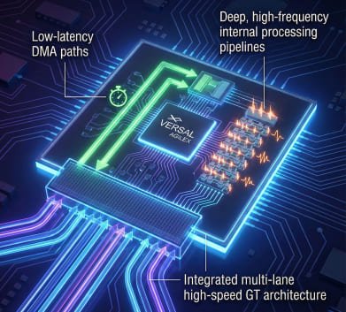
PCIe Gen5/Gen6 Endpoint on Leading FPGAs
Highlights:
- Integrated multi-lane high-speed GT architecture
- Low-latency DMA paths optimized for fast data movement
- Deep, high-frequency internal processing pipelines
Use-case: HPC interconnects and data-movement accelerators
Visual: block diagram (Host ↔ PCIe ↔ FPGA ↔ Memory)
JESD204C Transmit/Receive Pipeline
Highlights:
- Deterministic lane synchronization and latency control
- Integrated digital front-end processing and framing logic
- Fully timing-closed operation at multi-tens of Gbps
Use-case: RF front-ends and advanced 5G/6G PHY development
Visual: ADC → JESD Rx → FPGA Processing → DMA

Real-Time Vision Pipeline (FPGA + SoC Hybrid)
Highlights:
- End-to-end sensor ingestion through ISP and ML acceleration
- Robust timing closure across multiple clock domains
- Modular, reusable architecture suitable for ASIC migration
Use-case: Edge AI, robotics, and autonomous platforms
Visual: Sensor → FPGA → ARM cores → Output

Multi-Protocol Video Processing (ARINC/DVI/Display)
Highlights:
- Seamless handling of heterogeneous video protocols
- High-throughput scaling and color-processing pipelines
- Deterministic frame delivery within real-time deadlines
Use-case: Mission electronics and cockpit display systems
Visual:video protocol blocks with arrows

Architect and Build Your Next FPGA & SoC Platform With Us
From high-bandwidth data movement to real-time processing pipelines, we build FPGA and SoC platforms that meet performance and reliability targets.